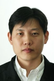
Seung-Joon Paik

Seung-Joon Paik's profile picture
seung.paik@ien.gatech.edu

Seung-Joon Paik received his B.S. degree at the School of Electrical Engineering in 1999 and the M.S. and Ph.D. degrees at the Electrical Engineering and Computer Science from Seoul National University, Seoul, Korea, in 2001 and 2005, respectively. His doctorate research focused on the design, microfabrication and testing of silicon microneedles for neurophysiologic applications, including microfluidic channels and microelectrodes. He was with Automation and Systems Research Institute in Seoul National University, as a postdoctoral associate from 2005 to 2007, where he developed sensors and systems of Inertial Measurement Unit (IMU) for localization and locomotion of robots. After joining a spin-off company from the research lab, SML Electronics, Inc., in 2007, he led the process team for the 8-inch wafer-level packaging process and foundry manufacturing process of MEMS accelerometers and gyroscopes for mobile applications as a senior research engineer. In 2008, he joined the MicroSensors and MicroActuators Laboratory (MSMA Lab.) in Georgia Institute of Technology, Atlanta, Georgia. He has led the BioMEMS research group at the MSMA Lab as a postdoctoral fellow. The BioMEMS research group is dedicated to developing micro/nano needles and biosensors for drug delivery and electrochemical sensing. In 2013, as a research engineer II at the Institute for Electronics and Nanotechnology (IEN) in Georgia Tech, he oversees and coordinates lab sections for College of Engineering courses within IEN which provides instructions to students about CMOS transistor fabrication and MEMS fabrication. He has been teaching and mentoring junior-level research engineers and graduate students on design, analysis, micromachining processes, and technical writing and presentation at Seoul National University, SML Electronics, and Georgia Institute of Technology. In 2014, he also worked in Southern Polytechnic State University (currently, Kennesaw State University) as an adjunct professor and taught a course of Microelectronic Engineering and its labs.

He has published 65+ reviewed journal and conference papers, and invented 13+ patents in USA and Korea, and has been a reviewer for the following Journals – IEEE Journal of Microelectromechanical Systems (JMEMS); IOP Journals of Micromechanics and Microengineering, Nanotechnology, Material Science and Technology, Journal of Physics D, and Smart Materials and Structures; and Sensors and Actuators A: Physics. His current interests are in research and development for the micromachining of silicon and polymer materials and in biomedical applications of micromachined devices and also in inertial sensors, 3-D multi-chip packaging of MEMS devices, energy storage/conversion devices and nano-scale structures.


Teaching Lab Coordinator
Research Engineer II
Phone
404.894.8807
Office
Pettit 205
University, College, and School/Department

Yolande Berta

Yolande Berta's profile picture
yb4@gatech.edu

Yolande Berta has over 30 years experience in electron microscopy, including both SEM and TEM. Berta has received equipment grants from the National Science Foundation and the Office of Naval Research. She has trained thousands of electron microscopy operators. Berta has a Master’s degree in Science from the School of Materials Science and Engineering at the Georgia Institute of Technology and a Master’s degree in Biology from the University of Illinois, Champaign-Urbana. 

As the Interim Director of the Responsible Conduct of Research (RCR) Program, her responsibilities include overseeing the RCR Academic Policy for Doctoral Students and the RCR Academic Policy for Master’s Thesis Students, teaching RCR courses for graduate students, and hosting RCR workshops.

Berta has more than 15 peer-reviewed publications and has given over 15 professional presentations.

Principal Research Scientist
Electron Microscopy Coordinator
Interim Director, Responsible Conduct of Research (RCR) Program
University, College, and School/Department

Mikkel Thomas

Mikkel Thomas's profile picture
mikkel.thomas@ien.gatech.edu

Mikkel A. Thomas has worked for the Institute for Matter and Systems since 2008. He earned a Bachelor of Science in Electrical Engineering in 1997, a Master of Science in Electrical Engineering in 1999 and a Ph.D. in Electrical Engineering with a specialization in Optoelectronics in 2008, all from the Georgia institute of Technology. Prior to his employment at Georgia Tech, Thomas worked at OptiComp Corporation located in Zephyr Cove, Nevada. His research at the company revolved around the development of VCSEL based, integrated optical communication systems for use in satellites and other aerospace applications. Since arriving at Georgia Tech, in the IMS, Thomas has provided cleanroom processing support to the academic faculty and their graduate students. He also provided processing support and fabrication services for entities not directly affiliated with the institute. Additionally, he was the lab instructor for ChBE 4050. In 2022, Thomas was named the Associate Director for Education and Outreach in IMS. In this role, Thomas is responsible for all the outreach efforts of the IRI covering K-Grey. He also organizes all the education coordinators in the National Nanotechnology Coordinated Infrastructure (NNCI) as part of his role in the NNCI coordinating office located at Georgia Tech.

Associate Director for Education and Outreach
Senior Research Engineer
Phone
404.385.8536
University, College, and School/Department

Walter Henderson

Walter Henderson's profile picture
walter.henderson@ien.gatech.edu

Walter Henderson manages a group of 8-10 research professionals that annually trains and helps ~700 researchers to perform 25000+ hours of work that enables ~$30M in research funding to Georgia Tech. 

He has significant experience in the growth, fabrication, and especially the characterization of microelectronic and nano-scale materials and devices. Henderson has been involved in this type of research since 1998 at all levels from vacuum system design and assembly to data analysis to paper and proposal writing/submission. 

Henderson has been an author on more than 30 publications in refereed publications such as the Journal of Applied Physics. His long-term goal is to move into education policy or public policy at the local or state level. 

Associate Director, Materials Characterization Facility
Principal Research Scientist
Phone
404.894.4702
Additional Research

Specialties: Structural, chemical, electrical and optical characterization of microelectronic, bio- and nano-technology materials and devices. I have designed hardware and software for - and/or instructed others on the use of - analysis techniques including but not limited to: SEM, XPS, XRD, AFM, SIMS, Raman, PL, Hall, IV, and CV.

Google Scholar
https://scholar.google.com/citations?hl=en&user=Sp--xe8AAAAJ&view_op=list_works&sortby=pubdate

David Gottfried

David Gottfried's profile picture
dsgottfried@gatech.edu

David Gottfried received a Bachelor of Science in chemistry (highest distinction, highest honors) in 1984 from the University of Michigan and continued his studies in physical chemistry at Stanford University under a National Science Foundation graduate fellowship, obtaining his Ph.D. in 1991. He then was a European Molecular Biology Organization post-doctoral fellow at the Weizmann Institute of Science/Bar-Ilan University before beginning research and teaching in biophysics at the Albert Einstein College of Medicine. In 1999 he moved to the Georgia Tech Research Institute where he designed and tested optical sensors for chemical and biological agents with food safety, environmental, and homeland security applications. Gottfried joined the Microelectronics Research Center in 2007, where he was a technical liaison and biomedical domain expert for the NSF-funded National Nanotechnology Infrastructure Network. Beginning in 2012 he served as a member of the Advanced Technology Team in the Institute for Electronics and Nanotechnology (IEN) and then was appointed Senior Assistant Director for IEN Nanotechnology Technical Programs in 2016. He is currently the IMS Associate Director of External User Programs, Director for the Southeastern Nanotechnology Infrastructure Corridor (SENIC), a member site of the National Nanotechnology Coordinated Infrastructure (NNCI), and Director for the NNCI Coordinating Office. Gottfried was selected as a Fellow of the American Chemical Society in 2012 and the American Association for the Advancement of Science in 2018. In 2021 he was named a Regents' Researcher by the Board of Regents of the University System of Georgia.

Regents' Researcher and Associate Director of External User Programs
Director, NNCI Coordinating Office
Director, SENIC
Phone
404.894.0479
Office
Marcus 1141
Additional Research

Point-of-Care DiagnositcsChemical and Biological SensorsInk-jet Printing & Applications

University, College, and School/Department
Google Scholar
https://scholar.google.com/citations?hl=en&user=Kaufn_oAAAAJ&view_op=list_works&sortby=pubdate